Tuesday, April 26, 2011

The Official Version of the DEV.BO (2.0)

Version 2.0 of the DEV.BO is now for sale in my online store!

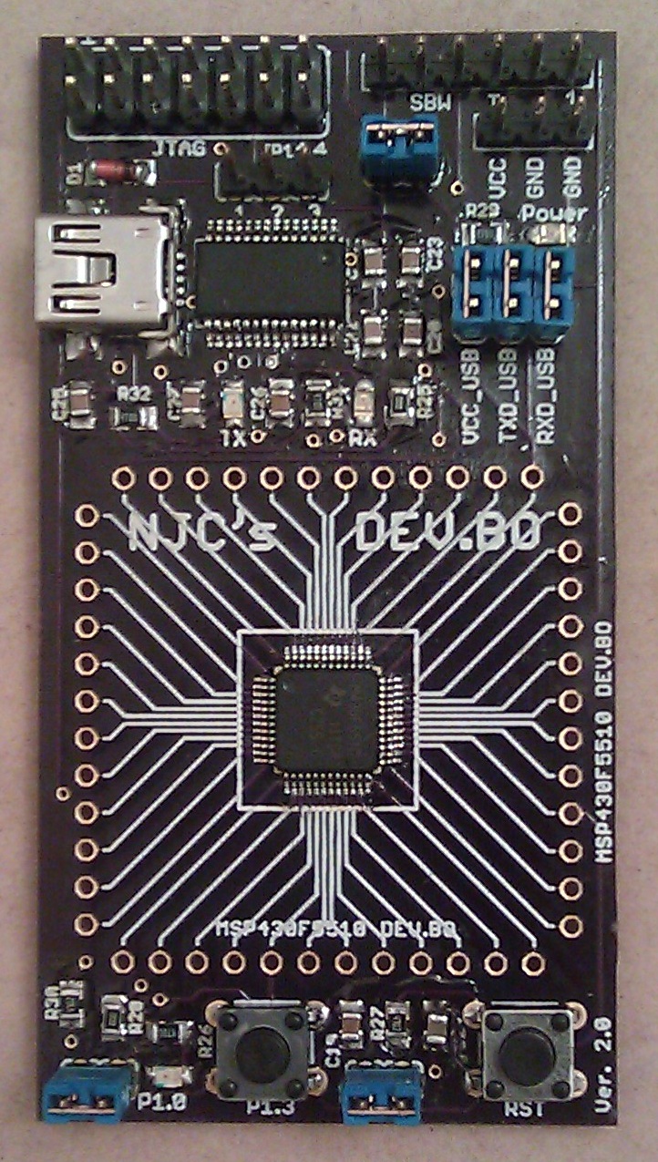
The DEV.BO is a development board based off of the MSP430F5510. This board can easily be programmed using the LaunchPad or any MSP430 JTAG programmer. Click here to see the post on the older DEV.BO.


DEV.BO Ver. 2.0 - Please ignore the flux residue on the board. I am out of flux remover and am expecting more in the mail soon.


Features and Specs
  • Based on the MSP430F5510
    • Max clock speed of 25MHz
    • Integrated 32kHz crystal
    • Broad supply voltage range - 1.8 V to 3.6 V 
    • 25K of flash memory
    • 1 USCI_A (UART/LIN/IrDA/SPI)
    • 1 USCI_B (I2C/SPI)
    • 2 16-bit (3CCR), 1 16-bit (5CCR), 1 16-bit (7CCR)
    • 10-bit SAR ADC
    • Internal temperature sensor
    • Hardware multiplier
    • Much more!
  • Connectors for both SBW and JTAG
    • The SBW is made for easy connection to the LaunchPad
  • USB interface (FTDI323RL)
  • On board reset button
  • 1 programmable push button
  • 1 programmable LED
  • Easy to use jumpers for disabling all non-mandatory circuitry
  • Extra power connectors for expansion boards

Available Documentation

Bare PCB (Unassembled) - $15

If you have all the tools you need to solder one up yourself, already have an MSP430F5510 from TI's free sample program, and all of the other parts needed, you can buy just the bare unassembled PCB. The handling time will also greatly reduced if you buy the bare board. Please note, that if you select this option, you will receive no components, you will only receive the PCB.


Without FTDI USB (MSP430 Assembled) - $35

This option is for those of you who do not need USB communication abilities and just want to use the MSP430F5510. If you select this option, you will receive a mostly assembled PCB. Everything needed to program and use the MSP430F5510 will be soldered onto the board but everything relating to the FTDI USB circuit (including the USB connector and the FTDI jumpers) will not be soldered to the board, and the parts will not be included. Male headers are also provided to connect to the MSP430's pins (the headers will not be soldered onto the board).


Full Board (Assembled) - $45

This option comes with everything already soldered onto the board. Male headers will also be included to connect to the MSP430's pins, but they are not soldered onto the board.


Example Code

Every DEV.BO which will have the MSP430 F5510 soldered onto it (Options: Without FTDI USB and Full Board) will come with a modified version of the LaunchScope code which samples at a rate of 4kHz. This code will be released as it's own post in the upcoming weeks once I have a chance to fully document it.

A New DEV - The DEV.BREAK

The second product available in my new online store is the DEV.BREAK! This board is simply a breakout board for the MSP430F5510 (or really any other chip with the 48LQFP package).

Do you want to build a small project on a breadboard with one of the most powerful MSP430s out there? Then this board is for you!

The bare DEV.BREAK PCB
This board doesn't require much explanation as it just breaks out all of the MSP430F5510's pins to a breadboard-able size. In a standard breadboard the DEV.BREAK leaves room for one row of wires on each side.

Purchasing Options

There are two options when purchasing this board. The first is to simply purchase the bare PCB for $9 with no chip soldered on, you will receive only the PCB (no MSP430 or headers). The second option is to buy the PCB with the MSP430 soldered onto it with headers included (but not soldered) for $20.

Tuesday, April 12, 2011

Housekeeping and a Store

I have just finished created a page which lists the most popular and important past posts. There are many times where I am asked a question on a newer posts which I answered at length in a previous post. Hopefully this page is found to be useful for many of you. If you find any typos anywhere, please let me know. As always, feel free to contact me via email: webmaster at msp430launchpad dot com.

Lately I have been putting my efforts into updating the look and feel of my blog to make it a bit more reader friendly. There is still much work to be done to make the new template really look and feel good, but I feel like I have made a lot of progress on organizing the blog and getting ready for the future.

One of the things which I have been working on behind the scenes, is a small web store where I will be selling a few boards I have created. This includes the DEV.BO, which I wrote about here, and a few other simple breakout boards which are pertinent to the LaunchPad and the MSP430.

Let me know what you think and stay tuned...

Wednesday, March 23, 2011

Appearance Change

I finally got around to changing the template for the blog since I was not happy with how the old version looked. Now everything should be a bit easier on the eyes and hyperlinks show up much better now.

Please let me know if there is anything I forgot to change or something else that I did not notice. Hope you like it!

Sunday, March 20, 2011

The DEV.BO is Born!

I would like to introduce you all to the DEV.BO prototype. This board is built around the MSP430F5510, it not only includes the typical on-board items, but also an FTDI chip.

The Dev.BO
As I have mentioned in previous posts, I was using the MSP430F5528 in a personal project of mine (which I will be posting when I have more time). TI just released a new set of chips in the MSP430F55xx series, one of which caught my eye, the MSP430F5510. This chip has all of the features I needed the 5528 for, but is half the price! Granted the 5510 does has less memory and a less precise ADC (and is lacking a few other things) but this was not important to my project.

Note: The MSP430F5510 on the DEV.BO is the 48 pin version which has a bit less peripherals than the larger sized MSP4305510 package.

I needed to get a board made for my project and decided to just go ahead and make a small target board which I might start selling if all goes well. Keep in mind this just a prototype and I need to test at least one more version before I can start selling them.

Some DEV.BO’s Features
  • Based on the MSP430F5510
    • Max clock speed of 25MHz
    • Integrated 32kHz crystal
    • 25K of flash memory
    • 1 USCI_A (UART/LIN/IrDA/SPI)
    • 1 USCI_B (I2C/SPI)
    • 2 16-bit (3CCR), 1 16-bit (5CCR), 1 16-bit (7CCR)
    • 10-bit SAR ADC
    • Much more!
  • Connectors for both SBW and JTAG
  • USB interface (FTDI323RL)
  • 1 programmable push button
  • 1 programmable LED
  • Much more!
DEV.BO size comparison
As you can see in the picture above, it is quite small. For me, it replaces the MSP430F5528 target board on the right and the FTDI breakout board from SparkFun on the upper left.

I am still here and working hard, sorry that my last posts have been quite sporadic. I love how the DEV.BO came out and am excited to get it more finalized in the upcoming weeks. It makes programming the 5510 a breeze because of how simple it is to connect to the LaunchPad. I was very frustrated with my MSP430F5528 target board and how many wires I needed to get things up and running. Mouser just got the MSP430F5510 (in the correct package) in stock, so I can start pushing things along.

The reason I wanted to post this now was because my next two posts will be about one of my latest mini projects - a heart beat detection algorithm implemented on an MSP430F55xx. Once I finish those posts I will delve into the details of I2C because it can be a very confusing topic for beginners (and even advanced developers!).

Sunday, January 9, 2011

Getting a PCB Made

I was recently asked where I get my PCBs made and realized that many people do not know of the great online PCB services which are available to hobbyists.

A few months ago I needed to get a PCB made for the first time in years and started the search for cheap places to get my board manufactured quickly with reasonable tolerances. I needed small quantities of a duel layer, surface mount, board with solder-mask and silkscreen on both sides. This usually adds more money to a PCB order than I was willing to spend on my small quick prototype board.

I found three services which met my cost requirements and did not have an unreasonable lead time. Here are my thoughts and a review on the PCB service I used.

MakePCB.com

http://makepcb.com/

This was the first board house I found which has reasonable pricing and a simple online quote system that you do not need to sign up for. I hate those websites where you have to give your personal information in order to receive a quote. This option seemed to be the best for me while I was living abroad since shipping to Europe was the same as the US. I ended up not using this service because there was no information on the website about how long it takes get your board. The major benefit to using this service is that if you want medium sized quantities the pricing scales very well. Check out their online quote calculator.

If anyone has used this service, send me a note or comment here. I'm very interested to see if anyone has had a good experience with this board house.

BatchPCB

http://batchpcb.com

This is a service run by SparkFun electronics and seems to be a great option when you do not need a board quickly. As with MakePCB, I ended up not using this service. On their FAQ page they say that it takes anywhere from 3 weeks to 4 weeks to receive your board. For the price this is very reasonable - considering most hobby projects are usually not time critical. One great feature of this website is that they save your board design and you can get new boards made at less cost;  you can even sell your designs!

The pricing is "$10 setup fee (shown as a handling charge) - $2.50 per square inch for 2 layer designs". This makes the pricing better for larger boards than the last service I mention here.

This site has great reviews from a multitude of people. Check out this forum for more reviews and information on the service.

Dorkbot PCB Group Order

http://dorkbotpdx.org/wiki/pcb_order


This service works in a similar way as BatchPCB does. The person who runs the website fills up a large panel with multiple orders from hobbyists in order to keep costs very low. They are very helpful and answered all the questions I had; they also check to make sure your design is saved in the right format for their process and the boards are spaced properly. They send the boards out as soon as a panel fills up or a certain date has passed. Recently the boards have been filling up quickly and there has been more than one order per month.


This service is great for very small sized boards, which is a major reason I used this site for my boards. My board size was slightly more than 4 square inches and my design was ready a few days before the panel was due to go out. The overall lead time once the panel is sent out, is about 2 weeks. This works great if you can plan to have your board ready a few days before the panel goes out.


I received three copies of my board which can be seen in the previous two pictures. The solder-mask was purple (which looks awesome by the way), the silkscreen is clear and readable, and the boards work perfectly! The build quality was spectacular and I am very impressed. I HIGHLY recommend this service to anyone who wants a PCB made. Like BatchPCB they also have a 4-layer service. International shipping is also very reasonable.

I also wanted to thank Doc for telling me about this service. As you can see by his blog post, it is very important to double and triple check a design before it is sent off to the board house. :-)

Final Thoughts

On a side note, my larger board (which can be seen in the pictures above) does have an MSP430 on it. The design uses a MSP430F2013 with the GND, RST, and TEST pins brought out through headers for programming.

I hope some of you find this information useful and possibly end up turning one of your small projects into a real permanent "product". It's very rewarding to see one of your designs working on a PCB. If you have used any other great cheap services, comment away.

Thursday, December 23, 2010

NJC's LaunchScope (A LaunchPad Oscilloscope)

After getting caught up on 43oh.com I am ready to get back to work! For all of you who have been patiently waiting for the final post in the oscilloscope project, it is here. I introduce to you, the LaunchScope. In this post I will present the code for implementing an oscilloscope (a slow oscilloscope) using only the LaunchPad and the MSP430G2231 that comes with it, in addition to providing the source code for the computer application I wrote to go along with the hardware.

Background

I originally built this project a few months ago for the MSP430F5528 for testing my own project which involved data acquisition of biomedical related signals. The 5528 has a built in USB and as such I could use a reasonably high sample rate; when using the LaunchPad though, one is seriously limited by the speeds at which you can transmit data out. As I've mentioned in one of my other posts, it's possible to use the SPI as a quasi-hardware UART for high speed transmission; this would allow you to use a much higher sample rate.

There is very little code on the microcomputer that needs to be added from the last post, all that is missing is the code for continuous reading of the analog channel. In addition to the functions needed for starting and stopping the ADC, the start and stop codes sent to the chip need to be handled.

The last post implemented a speed test which shows you how fast your setup is capable of transmitting data; this value will be used to determine the sample rate of the microcomputer. It is important to not sample at a rate higher than you can process the data because in addition to timing troubles you will end up missing and dropping samples, which could be detrimental depending on the application. Additionally, the code presented in last post can measure a single channel’s voltage using the MSP430F2231; the channels measured were one external channel (A3), the internal temperature sensor, and the internal VCC measure.

I was asked a question in a comment on my previous post, where the analog pin A3 is and I would like to explain that a little bit here before we get started. Almost every pin on all of the MSP430s have multiple functions, these functions can be found in the chips datasheet (not the family guide). For the MSP430F2231 which is the chip used with this series of posts, this can be found on page 6 in the datasheet. Here we can see that in the 14 pin version of the chip pin 5 is not only P1.3, but also ADC10CLK, A3, VREF--, and VEREF. The explanations of each purpose is also included in this table. The datasheet is one of the most useful resources you will have; everyone should have the datasheet and family guide easily accessible during development.

The Computer Application

Find the .zip file of my project here.

Find just the install for the application here. (Note: No promises that this will work for you)

I have decided to post the source code for my computer application since I know how useful it might be to many of you. The reason I was hesitant to post the code is because I do not document and comment my C# code as well as I do my MSP430 code. For anyone who downloads and uses my C# application, please do not expect well documented and commented code, though I will do my best to answer your questions on the 43oh.com/forum. Also, as with all of my code I ask anyone who uses it to mention in the code and anywhere it may be published or posted to site my blog and give me credit for whatever I have written. This includes the software UART and any other functions which I have specifically written.

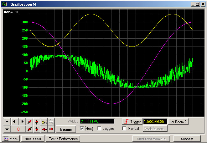
The computer application looks the same as the one I posted previously, except now the streaming buttons are not greyed out. The main difference is the oscilloscope code which will display a waveform in real time on the screen quite beautifully. Back when I needed this code for my own project I was writing my own library for displaying the waveform but was never happy with the results. I found this DAQ32datalogger project online which utilized Berstein's library for real time waveform displays. The first link was for a research project  testing the use of multiple accelerometers for replacing gyroscopes in real world applications. I was very impressed with his code and really recommend that you all take a look at his YouTube video which he links to on his site. The project utilized 32 accelerometer channels and displays all of them in real time on his PC. I emailed the author a few months ago and he is happy that his code is being utilized by others. If you use this code, PLEASE give credit where credit is due, his and Berstein's code is amazingly useful and helpful.

It is important to note that this library has much more potential and can do so much more than I use it for here. Eventually I plan on using this code for monitoring multiple bio-potential signals in real time. The image below is taken from Berstein’s website.


Note: I will not be discussing how this code works because this is a LaunchPad blog and not a C# blog. I am posting this code for those who already know C# or would like to change bits of the source code for their own projects. Keep in mind, this software is far from a polished program, I am using this for my own personal projects and wanted to share it with all of you. 

The Code

Also posted here on github.


Setting up the ADC and the Sample Rate

What will look the most unfamiliar to someone who has followed my blog up till this point is the streaming ADC function Start_Stream(unsigned int chan), here I set all the necessary values for the ADC stream. There should be only two lines which are unfamiliar to you which I used in this function.

ADC10CTL0 = ADC10ON + ADC10SHT_3 + MSC+ ADC10IE;
ADC10CTL1 = ADC10SSEL_3 + chan + ADC10DIV_7 + CONSEQ_2;

The first line will, turn on the ADC, set the sample and hold time to 64 clock cycles (which can be thought of as yet another divider for the ADC sample rate), sets the device to do multiple samples and conversions, and finally enables the interrupt. The second line selects which clock to use (the SMCLK), sets the channel to use (which is the ‘chan’ input from the function), sets the clock divider to SMCLK/8, and finally tells the ADC to sample a single channel consecutively.

As I already mentioned, it is important to make sure the sampling rate is low enough for the application UART to send every sample to the PC. Using my code the speed test on my application showed 6.21 kbps. Due to the fact that we are using an ADC that has a 10 bit vertical resolutions, we will need to send every sample as two bytes thus sending 16 bits of data per sample. So to calculate our max sample rate (which we should be a bit under just in case), we divide our data rate by our bits needing to be sent per sample, 6.21kbps / 16 bits = 397.44 Hz.

EDIT (01-26-2012): I would like to correct a mistake that was found in the following paragraph by one of my readers. The  problem is with the calculated sample rate. Instead of the equation being SMCLK/8/64/13, it should be SMCLK/8/(64+13). This is because the sample and hold time and the conversion time add together, determining the number of clock samples needed per conversion. This gives us a sample rate of approximately 1.6kHz, a value significantly greater than it should be. That being said, the code will still function, the reasons behind this is a bit complicated and won't be discussed here. Just know that some samples are being dropped and the actual transmission rate is closer to ~450 samples per second. Expect to see a new post in the future with updated code. Sorry for the error!

Our sample rate as set it in the Start_Stream() function is SMCLK/8/64/13. The 8 comes from the clock divider, the 64 comes from the sample and hold time, and the 13 comes from the number of clock cycles it takes to do an actual conversion. This value can be found in the datasheet on page 32 under “10-bit ADC, timing parameters -- MSP430G2x31 only”. SMCLK = 1000kHz (1MHz), so our sample rate is 1000/8/64/13 = 0.150kHz or 150Hz. This is much less than half of our maximum, so we are well within the limit of safety.

ADC10CTL0 &= ~ENC;
ADC10CTL0 &= ~ADC10SC;
ADC10CTL0 &= ~ADC10ON;

These three lines of code are what make up the Stop_Stream() function. It is important to note that ENC needs to be cleared first before any of the other values in ADC10CTL0 can be written. Once that is cleared, the conversion is stopped and the ADC is turned off to save power.

Why Have Commands?

Why not just make the chip constantly send out the data stream of the analog channel conversion results? All we want is an oscilloscope, so why need all of these weird command things? First, if you wanted to do that you would not use an MSP430 but rather you would use a nice and cheap ADC that has a UART out. We also have a built in temperature sensor, and internal VCC measurements which allow us to know almost exactly what voltage is being read by the ADC. Second, it is much easier to interface with a computer application when the program has control over the data flow. Without these commands the application would have a hard time making sure all the data is being received correctly and would not be able to read any of these other nice values the MSP430 can provide.

Improving the Design 

The biggest improvement which I’m sure everyone would like to see is an increase in sampling speed. I will not be doing a post on a faster scope design because it should be very easy to scale this code to faster speeds. If you decide to use an FTDI chip instead of the application UART you can recalculate the maximum speed the software UART can transmit at, then reconfigure the ADC to sample at a certain speed using the method I used in this post. If you would like to use an MSP430F5528 to increase speed, send me an email and I can send you the original source code this project was build from.

Final Thoughts

I hope you all enjoyed this series and find the LaunchScope useful. I have been and will be very busy in the upcoming months since I am leading a “Senior Design” project for my university. The project does utilize multiple MSP430s and I will be doing my best to post more guides on topics which come up during the course of my work.

Before I finish I have an unrelated question for any of my readers which might have experience with Actel FPGAs. I am thinking of using an Actel FPGA for a project and was wondering if anyone has had any experience with Actel FPGAs. I have only used Xilinx and Altera but saw that Actel has very cheap and low powered FPGAs. Any opinion on Actel chips would be greatly appreciated. Email me, webmaster@msp430launchpad.com.

Again, sorry for the delay, but I hope the wait was worth it. When I get around to it, the next post will discuss communication between two (maybe three) LaunchPads using I2C. If you have any simple questions about the post feel free to comment and I will do my best to answer any questions. If you have a complex question or would like some help with your code check out 43oh.com/forum, they have a great forum which I check when I can.

As always, comment away! Let me know what you think of the project. If you used the LaunchScope or the code from this series for anything cool, post a comment about it. Stay tuned, I will be writing more posts.