Thursday, October 27, 2011

Programming the DEV.BO and External Targets with a LaunchPad

Many readers have been asking me how to program the DEV.BO with the LaunchPad. Likewise, many of you are also wondering how to program the newer MSP430 microcontrollers with the LaunchPad, such as the MSP430F55xx series.

Since this seems to have sparked quite a bit of confusion, I want to make this post complete and thorough. There are two ways to program an MSP430: the first is using four-wire JTAG, the second is using two-wire JTAG. The LaunchPad can only use the two-wire JTAG method, which is also known as Spy-Bi-Wire (SBW). For the rest of this post, I will be referring to the two-wire JTAG as SBW and four-wire JTAG as just JTAG.

I want to make sure this is clear before I continue; JTAG and SBW are two separate methods for programming an MSP430. The LaunchPad can program MSP430s using SBW, not JTAG. That being said, not all MSP430s can be programmed using SBW, some of the older MSP430s can only be programmed using JTAG. TI has a document, SLAU157, which shows which chips support either just JTAG or both JTAG and SBW.

Now that we know JTAG and SBW are different methods of programming newer MSP430s, how do we use the LaunchPad to program all these cool devices? Spy-Bi-Wire needs two wires to program an MSP430: RST and TEST. The image below shows where you can find these two pins on the Launchpad.
The programming pins on the LaunchPad
The RST pin is shown by a yellow square, TEST is shown by a green square, and all of the GND pins are shown by blue squares. What about power? Well, you can either use the LaunchPad to power the DEV.BO (or your target MSP430 that supports SBW) or use an external power source. Regardless of how you power the target, you will need to also connect the LaunchPad's GND pin to the target. This is because you need a common reference for the data pins (RST and TEST); so technically you actually need a minimum of three wires to program an MSP430.

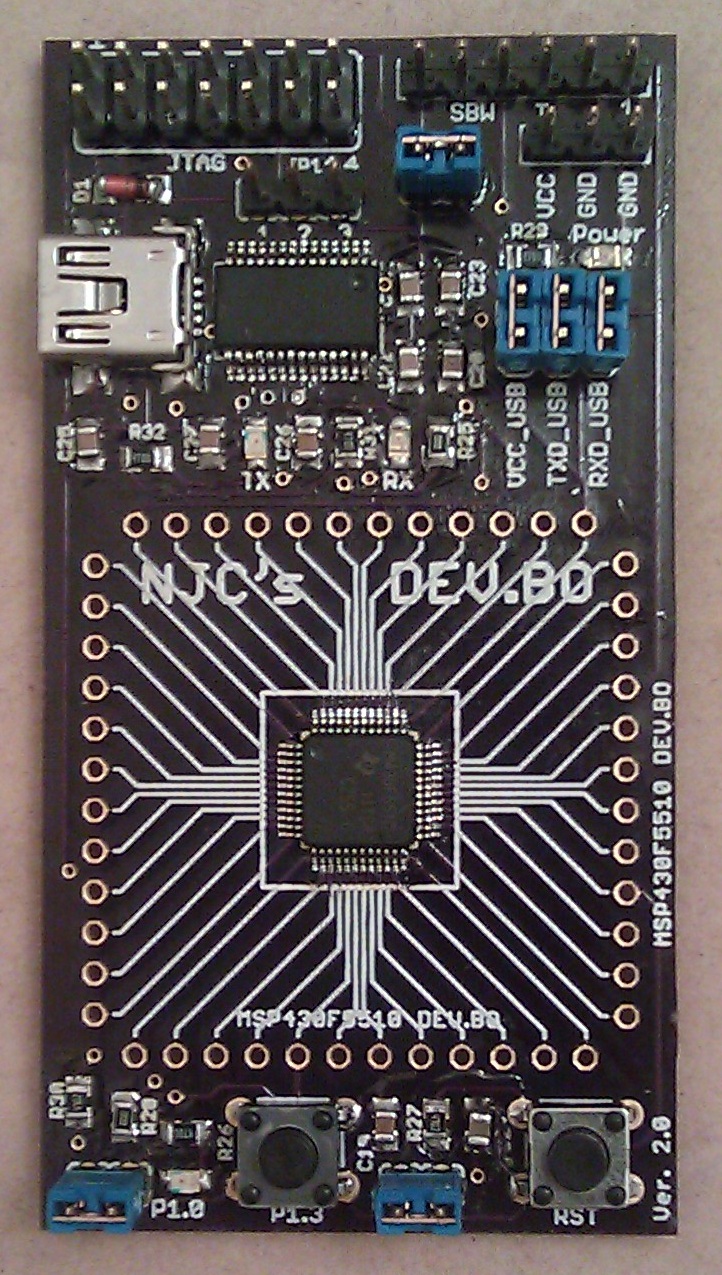
DEV.BO programming header
For this post we will use the LaunchPad to not only program the DEV.BO, but to also power it during programming. The image above shows which signals make up the programming header on the DEV.BO. There is a reason that I designed the programming header pins in that order. They are the same order as the LaunchPad; this is very important. What about the GND pin on the LaunchPad? Though there is no GND pin on the programming header, the LaunchPad does have a few GND pins available on board. Depending on what you have to connect the boards together, determines which GND you should choose.

The programming connection on the LaunchPad's side
The image above shows how I connect the DEV.BOs header to the LaunchPad. That nice six pin rainbow connector is available here at SparkFun and it works great for this task. Notice how I am using female connectors on this LaunchPad which makes it easy for me to connect GND to the rainbow connector using just a short breadboard wire. If you don't have access to this nice rainbow ribbon cable, you can use any method to connect these pins together.

Hopefully that should clear up any confusion on how to program the DEV.BO. Using this method, you can also program any other MSP430 that supports SBW; just connect up the necessary pins and you can program away.

I have two last things I want to mention. The RXD and TXD pins are not needed for programming but I included them on the DEV.BO in case they are ever needed for a project. The second thing is that you need to make sure the correct chip is selected in CCS or whatever IDE you use when programming the MSP430, otherwise it probably won't work.

I hope this clears up any confusion on how to program external MSP430s, including the DEV.BO, using the LaunchPad. Please leave a comment if you have any questions about this post. Don't forget to check out the DEV.BO, which is available in my online store.

Comment away!

Wednesday, October 26, 2011

Bluetooth Breakout and Free Shipping

I would like add yet another product to my online store, NJC's Bluetooth breakout board. I would also like to announce that there is now free shipping on all orders within the contiguous United States for items on my online store.

This board is based off of the RN-42 module which is very easy to use and add to your current projects. A few weeks ago I actually wrote a post on how to add Bluetooth to your MSP430 project that mentioned this breakout board. The circuit board is a modified design of SparkFun's Bluetooth breakout board which adds status LEDs and all the passive components needed to make this board "plug and play" right into your project while keeping all the important yet non-essential pins available. The module is also small enough that it can be added to existing projects with ease.

Populated Bluetooth breakout board
You have two options when buying this board, either completely assembled or as a bare PCB. The completely assembled board is a good option for those of you who don't want to fuss with surface mount components, and want a guaranteed working board. The bare PCB is a great option for those of you who have no problem soldering surface mount components and who want to add Bluetooth to their project while spending as little as possible.

Top of the PCB with each pin labeled

The picture above shows the pinout of the board, which should make it very easy for you to incorporate into your project. You just need to connect the RX, TX, 3.3V, and GND to your project, and you are ready to go. The full schematic of the board can be downloaded below.

Interested? Pick one up at my online store!

Please let me know if you have any questions!


Documentation
RN-42 Datasheet
RN-42 User Manual
NJC Bluetooth Breakout Schematic

Thursday, October 13, 2011

Introducing the MAVRK

What is the MAVRK? MAVRK stands for Module and Versatile Reference Kit. It is a new hardware platform developed by Texas Instruments which will allow you to evaluate almost any configuration of Texas Instruments' products. I have been given the opportunity to evaluate this kit before it is released and will be generating content for the community. This post will introduce you to the MAVRK and give a brief explanation of what the kit is.

While I am still not sure who Texas Instruments is targeting with this board , I think that professionals, students, and hobbyists all will be able to find some interesting uses for this system.
MAVRK with two modules installed.
This is a picture of the MAVRK board with two modules installed. I think it's pretty cool looking!

Instead of trying to explain exactly what the MAVRK is, I will give you a scenario in which you would want to use the MAVRK. Imagine you want to build a quadcopter that can be monitored and/or controlled wirelessly from a nearby computer. Instead of taking lots of time and money building prototype after prototype till you get the design right, you can use the MAVRK. First you would need a motor module, a wireless module (say Wi-Fi for example), an MSP430 module, and a few analog or digital input modules. All of these things TI apparently plans on offering at quite low prices.

You would plug everything in to the motherboard, hook any accelerometers you have to the input modules, hook a few test motors up to the motor module, and start programming away. The MAVRK programming tool chain is supposed to make the integration of these modules easy and quick. If all goes to plan, you should have a working model within days, not weeks. Now all that is left is to take the MAVRK setup, and turn your working design into a custom PCB; this step should also be easy considering the MAVRK and all the modules are open source, including the hardware.

I will be started a separate blog about the MAVRK system which will go into more detail about the kit and how to get started with the kit. Stay tuned! Let's see what this baby can do!

Wednesday, August 24, 2011

DEV.BO on eBay

After receiving some emails from a few readers, I have decided to also sell some of my boards on eBay. I understand that this might be a more comfortable and care-free way of buying my boards. Currently I have posted a DEV.BO and will be posting some others soon (the list below will be updated as I post boards). If this works out well I will add other boards to my eBay account. Also, I will probably forget to remove the links when the items end; keep that in mind.

Click here for the DEV.BO!
Click here for the Bluetooth Breakout!

I have a few posts in the works but if anyone has a suggestion for a simple tutorial or guide, let me know.

Happy Bidding!!

Monday, August 8, 2011

Adding Bluetooth to your MSP430 Project

Most projects which I have seen input and output some sort of data: be it a multimedia stream, sensor data, or user inputs. In this post I will discuss how to easily make your project Bluetooth enabled. For hobbyists and professionals alike one of the most important aspects of any design is cost; in my own project I had three requirements for a Bluetooth Module, low cost, low size, and very easy to use.

The RN-42 module, which is available at SparkFun electronics and Mouser, is a very cheap and simple way to use Bluetooth in your project. The best part about the RN-42 module is that it has an integrated antennae and contains everything needed for the Bluetooth protocol. You would be surprised how many modules require a special external microcomputer that contains a Bluetooth stack to operate.

For how great the module may seen, there are a multitude of downsides. The first is not such a big deal and might not even be a downside for you. The device is in a surface mount package. For those of you who are not making your own PCBs, you can buy one at my online store and be done with it. For those of you on a budget, it is possible to solder wires onto each pad of the RN-42 even though I would not recommend it. The last, and my favorite solution, is to just make a custom PCB for your project and solder on the module yourself. The picture below is of a custom breakout board I made to evaluate the module. The schematic is shown later in this post.

My custom breakout board for the RN-42.
The other negative aspects of this module are its size and maximum baud rate. The module is a little bigger than I would like, but still reasonably small. The device also draws a bit more power than I would like, but all things considered it is not too bad for being a Bluetooth module. What bothers me the most about this device is that the maximum baud rate is very very low. I will discuss this in more detail after I show you how to integrate this device into your project.

Link Summary

RN-42 at SparkFun
RN-42 Breakout at SparkFun
RN-42 at Mouser
RN-42 Datasheet
Roving Networks User Manual
NJC's Software UART
RealTerm

Adding Bluetooth to your Project

The easiest way to send and receive data using this Bluetooth module is to use a UART connection. The first schematic below, which is based off of the datasheet and example schematic from SparkFun, is how I connected the module to my project.

A complicated example for hooking up the RN-42 to the MSP430F5510.
This shows how to connect the RN-42 to an MSP430. Please note that this is just an example and that it is much more complicated than the bare minimum; see the next schematic for the bare minimum needed. The first and most important thing I want to mention is that the device requires a supply voltage between 3V and 3.6V. Luckily I use 3.3V for most of my projects which is perfect for this module.

My custom breakout board for the RN-42
The figure above shows the schematic for the breakout board which I used for evaluating the device and shows what kind of connections the module needs in order to function properly. After testing the device thoroughly it was obvious to me that the device is so simple to use that I could have put it in my project right away. The range is quite good and the device is very reliable when using a baud rate of 115200.

Connecting

Hopefully by now it is clear that from the hardware side of things only a UART connection is needed between the Bluetooth module and your MSP430. What about from the other side of the data stream? The computer. Linking the module to the computer was surprisingly easy. On Windows 7 (I can’t speak for any other OS or version of Windows), it was plug and play. Within a few seconds the drivers were automatically installed and I could see which COM port the module was connected to in the device manager.

The device manager showing the RN-42 connected as COM6.
As I mentioned before, my terminal program of choice is Realterm. The first test I recommend completing when setting up the module is a simple echo test. Connect the RX and TX pins on the module together, then set the COM port to the correct port and the baud rate to 115200 baud in your terminal. Once everything is set up and the power is on, wait for the device to connect. If you have the status LEDs connected to the module (which are optional if you are worried about power consumption), the LED connected to PIO2 should turn on when the module is paired with the computer. The other status LED will blink if the device is not connected. Once connected, type a few characters in the terminal and you should receive back every character you typed into the terminal.

Note: If you are running off of a battery, which you probably are given that this is a post about Bluetooth, you will run into connection issues when the battery is getting low. The module will still turn on and the LEDs will still blink, but you will not be able to reliably connect. If you are having connection issues, check your battery.

That should be all that you need to know in order to add Bluetooth to your project. If you think there is something I have missed, let me know and I will add a section to this post.

Commands?

Yes, this module can accept commands which allow the user to change some important settings. I will not be discussing these commands in this post. You can find all the information you need on this topic in the Roving Networks User Manual.

Baud Rate Trouble

As I mentioned earlier I want to discuss the problems I have with the data rate of this device. My frustrations really arise from false claims on the specifications of the device from both the manufacturer and vendors. 
  • "Over air data rate of 721kbps to 2.0Mbps" - SparkFun product page
  • "Data Rate: 1200 bps to 921 Kbps" - Mouser
  • "Sustained SPP data rates - 240Kbps (slave), 300Kbps (master)" and "HCI data rates - 1.5Mbps sustained, 3.0Mbps burst in HCI mode" - Roving Networks Datasheet for the RN-42
The quotes above show where my frustrations originate. To be honest, I am not really sure where SparkFun got their numbers; if I am missing something, please point it out to me. To make things clear, this device really only functions in SPP mode, thus you have a max data rate of 240Kbps if the device is in slave mode. I'm not even sure if it's possible to put the device in HCI mode, apparently it must be done at the factory.

So the datasheet is clear about the max speeds in each mode, but I am frustrated that they do not make it abundantly clear that the device cannot work in HCI mode. I emailed Roving Networks inquiring about this dilemma I was having (I wanted to use 921600 baud sustained over the air) and though they were friendly, prompt, and reasonably helpful, I was/am not happy with how misleading their datasheets are.

“The HCI mode is a special build of firmware the needs to be programmed at the factory.” “Please understand that in HCI mode, the bluetooth stack is running on the external host processor and the module is acting as a radio.” All in all, I do commend them on their customer service, just keep in mind that realistically speaking, you will only be able to use SPP mode.

Conclusions

Despite my frustrations, this is a great solution for making your project wireless. I have found very few chips or modules that can be integrated into a project with such ease. I hope this post helps a few people successfully add Bluetooth to their projects. There are so many cool possibilities for projects when using Bluetooth; the possibilities are endless! Who wouldn't want to hook up a project to an Android phone?

Comment away! Let me know what projects you have added Bluetooth to!

Thursday, July 14, 2011

Update

It recently came to my attention that my webstore has not been working correctly. Instead of loading the shopping cart when an item was added, the PayPal homepage would be loaded. I believe that I have fixed everything, but please let me know if you have any more problems with the store.

I apologize to any of you who tried to place an order while the store was not working correctly.

For any inconvenience this may have caused, all orders placed in the next week will receive an automatic refund of 20% when the item(s) ship. This is valid from 07-14-2011 until 11:59PM-EST 07-21-2011.

Please let me know if you have any questions or concerns.

Tuesday, June 7, 2011

A Simple LaunchPad DAC

Here I will show you how to build a simple DAC using just the LaunchPad and a few common analog components!

It has been quite some time since I have posted some code and after all that has been going on I now have time to write a new technical post! Though I developed this mini-project on the MSP430F5510, I have ported it over to the MSP430G2231 so it can be implemented using just a LaunchPad and some common analog components. This project came about because I wanted to automate signal to noise testing on a product I am making and I did not have the money for a new controllable digital function generator. I needed a way generate a sine wave, then I needed to sweep across a certain small range of frequencies. At each frequency data would be logged and then analyzed in MATLAB.

Sounds complicated, but the principle is very simple. I wanted to build a digital to analog converter (DAC) using an MSP430 that can generate periodic waveforms. I came up with this concept and decided to build it mostly out of curiosity since I could have just bought a signal generator chip or high-speed DAC at a very low cost.

This post will show you how to generate a periodic analog signal using the LaunchPad and the MSP430G2231. For the sake of simplicity, I stuck to the default DCO value. This will allow us to generate a very clean sine wave at 128Hz. If the DCO is increased to 16MHz and a few other design parameters are changed the maximum frequency can be over 4kHz. Using the MSP430F5510 I was able to generate a crystal clear 32kHz sine wave.

Why would you want to do this? Well, this code can be modified so any arbitrary analog waveform can be generated (reasonably speaking). At the very least you will learn some interesting analog principles if you decide to build this mini-project.

How it Works

First I will start out with some theory. The goal here is to generate an analog sine wave (or any signal for that matter). An analog signal, or a continuous signal, is not something which a microcomputer easily works with unless there are analog peripherals to make the job easy. Even then, things are quite discrete. The figures below show a continuous sine wave, and a discrete sine wave.


Continuous Sine Wave
Discrete Sine Wave
This is very basic theory, feel free to skip ahead to the code. As you can imagine, the more discrete points per period, the more it looks like a continuous sine wave. The minimum points needed (theoretically) to represent a certain frequency is two (see aliasing). In order to have a clean representation of the signal though, quite a few more than two points are needed. For this post I have chosen to use 32 points per period to make a sine wave for the sake of simplicity. This actually can be reduced which will allow for greater speeds while maintaining very good signal quality.

Great, now we know how to make an analog signal from a few analog points, but how do we generate these analog points in time? PWM. If you are unfamiliar with PWM, please check out an old post of mine here and the wiki page. By using a digital PWM signal, an analog voltage can be generated which is determined by the duty cycle of the PWM. If you take the average voltage across a single period of PWM by using a capacitor (or low-pass filter) a range of analog values can be generated.

So now we can generate the 32 analog points of our sine by using PWM with a little bit of analog circuitry.

The Code

Before we get to the analog circuitry I thought I would discuss the code first. As always, the code is posted here on github and is embedded below.


First, I would like to discuss the sine wave look-up table which is at the top of the code. The array is called wave[] and consists of the 32 values we need to make a sine wave. It is important to note that even though we have 256 possible duty cycles when using 256 clock pulses per PWM, we never go above 192 or below 64 (for a range of 128). This is very important since all of the instructions which need to get executed every interrupt take clock cycles of their own. If the duty cycle interrupt happens before the other interrupt routine finished, a pulse is missed and the output signal becomes warped.

The code itself is quite simple because we are simply generating a PWM using interrupt routines. Again, if this code seems very foreign to you, please check out my post on PWM. The important difference between this code and the typical PWM code is that the duty cycle automatically is changed every period.

Every time a new period is started, the interrupt TIMERA0_VECTOR is thrown. Here will increment a counter which keeps place of our position in the sine wave array; we also will reset the counter as needed. The current value which we are going to be outputting is set to the Capture Compare Register 1 (CCR1). Though it is possible to clear or set the output pin without going into an interrupt routine, I thought it was important to show how the CCR1 interrupt is call because it is slightly different than CCR0.

A separate interrupt vector, TIMERA1_VECTOR, is thrown when the timer is equal to the value in CCR1. This is also the interrupt vector that is called for any other CCR registers that may be available on the MSP430 and overflows. For example, the MSP430F5510 has a timer with 7 capture compare registers! To determine which register threw the interrupt you must check the TAIV register. To see which bit corresponds to which capture register, see the datasheet for your device.

Other than that, if you have read my other posts, you should understand the code. If you have any questions, you know the drill.

The Analog Circuitry

The PWM signal will need to be average, or smoothed out. If the high frequency components are removed, only the average signal remains. Lets make a quick example before we get to the physical implementation on a breadboard.
Example Signal
The above image shows a rectified sine wave which is made up of multiple higher frequency sine waves (blue). This will allow us to visualize how filtering works. After filtering the signal using a low-pass filter, which allow only the frequencies lower than the desired rectified sine wave through; realistically it is not a perfectly sharp cutoff and a little low amplitude high frequency components remain. The result is shown above in green. If this is a bit hard to understand, do not worry, this is just some background theory for those who are interested. Now, let me show you what our actual PWM output will look like for a sine wave.


Actual Theoretical Output

The above image shows what our PWM output will actually look like. You can see that there are 32 separate PWM periods which make up the sine wave. Each PWM period consists of 256 clock ticks; thus the final sine wave consists of 32*256 =  ~8k clock ticks. The final sine wave output is also shown above in green. This is the result of filtering the PWM output signal. For those who are wondering, all of the graphs above were generated in MATLAB.

The Circuit

Great! Now we know how it all works, but how do we actually implement it. I will skip out on filter theory and just present you with a second order low-pass filter

Analog Circuitry
Above is the schematic for all of the analog circuitry that is needed. The analog output, when using the code show above, from the MSP430 will be centered at approximately half of the supply voltage. If we wanted to amplify the signal further, we would need a reference voltage for any amplifier circuitry. For this project we will not do that for the sake of simplicity.

Now onto the circuit. It consists of two passive, low-pass filters separated by two voltage followers (buffers). While it is possible to simply cascade the two filters without the buffers, buffers allow impedance matching; a topic which I will not discuss here. Each filter has a cufoff frequency of approximately 160Hz ( 1/(2*pi*10k*.1uF) ) which is slightly above the desired sine wave frequency of 128Hz and much less than the PWM frequency of 4kHz (1MHz/256 clock ticks).

Note: If you change the timing of the microcomputer to allow for faster or slower sine waves, you MUST also change the cutoff frequency of the low-pass filters.

The Results?

What does the output look like? This post wouldn’t be complete without some scope captures to show the actual results. I really love when the theory works out and the results can be seen easily. Understanding the theory behind not only digital systems, but also analog circuitry can be a huge help in all sorts of projects.
Actual PWM Output
The above image shows both the PWM output from the MSP430 and the sine wave output from the low-pass filters. Very cool! As you can see, the peak to peak voltage of the sine wave is less than the supply voltage (VDD, which is ~3.6V).

Sine Wave Output
The picture above allows you to better see the sine wave output which is 1V peak to peak and 131Hz; it sure looks great! To improve the results, some changes can be made to the project. Less points can be used per sine wave, thus increasing the maximum frequency generated. This makes the output more “jagged” but with correct filtering this would not matter. Further, if you want to increase the peak-to-peak voltage or increase the power for any reason, amplification can be used.

For all the scope measurements I used a Rigol Oscilloscope (DS1052E) which I discovered through the EEVBlog. It is an amazing scope for the price and I would recommend it to anyone. Personally I think it is much better than the really low end Tektronix which are much more expensive, and I much prefer this to older analog scopes.

Final Thoughts

What’s next? It is possible to change the frequency of the sine wave within the MSP430. This could also be the basis for an arbitrary digital function generated using the MSP430. The possibilities are endless! As always, if you have any questions please comment here or email me. If you want a more immediate answer (since I am busy and sometimes take a while to respond) post your question on 43oh.com/forum. Maybe one day soon I will combine the LaunchScope and this project to create a single, simple, controllable, single test board solution using the DEV.BO.

I hope that you found this interesting. I know you all will come up with many cool uses for this project, so please comment and let me know the cool ways which you use the code.

Tuesday, April 26, 2011

NJC's MSP430 Store Is Open For Business!

Today I opened my new online store! The DEV.BO is the first item in the store, and a breakout board for the MSP430F5510 called the DEV.BREAK is the second. The two posts before this one provide details of the two items. Please make sure you read the important information at the top of the store before you buy anything.

Now that the store has been opened, I will be writing more technical posts which show off some cool things the LaunchPad and other MSP430s can do.

Please note that all these prices are introductory and are subject to change. If you have any questions, please contact me via email: webmaster (at) msp430launchpad (dot) com.

Check it out!

The Official Version of the DEV.BO (2.0)

Version 2.0 of the DEV.BO is now for sale in my online store!

The DEV.BO is a development board based off of the MSP430F5510. This board can easily be programmed using the LaunchPad or any MSP430 JTAG programmer. Click here to see the post on the older DEV.BO.


DEV.BO Ver. 2.0 - Please ignore the flux residue on the board. I am out of flux remover and am expecting more in the mail soon.


Features and Specs
  • Based on the MSP430F5510
    • Max clock speed of 25MHz
    • Integrated 32kHz crystal
    • Broad supply voltage range - 1.8 V to 3.6 V 
    • 25K of flash memory
    • 1 USCI_A (UART/LIN/IrDA/SPI)
    • 1 USCI_B (I2C/SPI)
    • 2 16-bit (3CCR), 1 16-bit (5CCR), 1 16-bit (7CCR)
    • 10-bit SAR ADC
    • Internal temperature sensor
    • Hardware multiplier
    • Much more!
  • Connectors for both SBW and JTAG
    • The SBW is made for easy connection to the LaunchPad
  • USB interface (FTDI323RL)
  • On board reset button
  • 1 programmable push button
  • 1 programmable LED
  • Easy to use jumpers for disabling all non-mandatory circuitry
  • Extra power connectors for expansion boards

Available Documentation

Bare PCB (Unassembled) - $15

If you have all the tools you need to solder one up yourself, already have an MSP430F5510 from TI's free sample program, and all of the other parts needed, you can buy just the bare unassembled PCB. The handling time will also greatly reduced if you buy the bare board. Please note, that if you select this option, you will receive no components, you will only receive the PCB.


Without FTDI USB (MSP430 Assembled) - $35

This option is for those of you who do not need USB communication abilities and just want to use the MSP430F5510. If you select this option, you will receive a mostly assembled PCB. Everything needed to program and use the MSP430F5510 will be soldered onto the board but everything relating to the FTDI USB circuit (including the USB connector and the FTDI jumpers) will not be soldered to the board, and the parts will not be included. Male headers are also provided to connect to the MSP430's pins (the headers will not be soldered onto the board).


Full Board (Assembled) - $45

This option comes with everything already soldered onto the board. Male headers will also be included to connect to the MSP430's pins, but they are not soldered onto the board.


Example Code

Every DEV.BO which will have the MSP430 F5510 soldered onto it (Options: Without FTDI USB and Full Board) will come with a modified version of the LaunchScope code which samples at a rate of 4kHz. This code will be released as it's own post in the upcoming weeks once I have a chance to fully document it.

A New DEV - The DEV.BREAK

The second product available in my new online store is the DEV.BREAK! This board is simply a breakout board for the MSP430F5510 (or really any other chip with the 48LQFP package).

Do you want to build a small project on a breadboard with one of the most powerful MSP430s out there? Then this board is for you!

The bare DEV.BREAK PCB
This board doesn't require much explanation as it just breaks out all of the MSP430F5510's pins to a breadboard-able size. In a standard breadboard the DEV.BREAK leaves room for one row of wires on each side.

Purchasing Options

There are two options when purchasing this board. The first is to simply purchase the bare PCB for $9 with no chip soldered on, you will receive only the PCB (no MSP430 or headers). The second option is to buy the PCB with the MSP430 soldered onto it with headers included (but not soldered) for $20.

Tuesday, April 12, 2011

Housekeeping and a Store

I have just finished created a page which lists the most popular and important past posts. There are many times where I am asked a question on a newer posts which I answered at length in a previous post. Hopefully this page is found to be useful for many of you. If you find any typos anywhere, please let me know. As always, feel free to contact me via email: webmaster at msp430launchpad dot com.

Lately I have been putting my efforts into updating the look and feel of my blog to make it a bit more reader friendly. There is still much work to be done to make the new template really look and feel good, but I feel like I have made a lot of progress on organizing the blog and getting ready for the future.

One of the things which I have been working on behind the scenes, is a small web store where I will be selling a few boards I have created. This includes the DEV.BO, which I wrote about here, and a few other simple breakout boards which are pertinent to the LaunchPad and the MSP430.

Let me know what you think and stay tuned...

Wednesday, March 23, 2011

Appearance Change

I finally got around to changing the template for the blog since I was not happy with how the old version looked. Now everything should be a bit easier on the eyes and hyperlinks show up much better now.

Please let me know if there is anything I forgot to change or something else that I did not notice. Hope you like it!

Sunday, March 20, 2011

The DEV.BO is Born!

I would like to introduce you all to the DEV.BO prototype. This board is built around the MSP430F5510, it not only includes the typical on-board items, but also an FTDI chip.

The Dev.BO
As I have mentioned in previous posts, I was using the MSP430F5528 in a personal project of mine (which I will be posting when I have more time). TI just released a new set of chips in the MSP430F55xx series, one of which caught my eye, the MSP430F5510. This chip has all of the features I needed the 5528 for, but is half the price! Granted the 5510 does has less memory and a less precise ADC (and is lacking a few other things) but this was not important to my project.

Note: The MSP430F5510 on the DEV.BO is the 48 pin version which has a bit less peripherals than the larger sized MSP4305510 package.

I needed to get a board made for my project and decided to just go ahead and make a small target board which I might start selling if all goes well. Keep in mind this just a prototype and I need to test at least one more version before I can start selling them.

Some DEV.BO’s Features
  • Based on the MSP430F5510
    • Max clock speed of 25MHz
    • Integrated 32kHz crystal
    • 25K of flash memory
    • 1 USCI_A (UART/LIN/IrDA/SPI)
    • 1 USCI_B (I2C/SPI)
    • 2 16-bit (3CCR), 1 16-bit (5CCR), 1 16-bit (7CCR)
    • 10-bit SAR ADC
    • Much more!
  • Connectors for both SBW and JTAG
  • USB interface (FTDI323RL)
  • 1 programmable push button
  • 1 programmable LED
  • Much more!
DEV.BO size comparison
As you can see in the picture above, it is quite small. For me, it replaces the MSP430F5528 target board on the right and the FTDI breakout board from SparkFun on the upper left.

I am still here and working hard, sorry that my last posts have been quite sporadic. I love how the DEV.BO came out and am excited to get it more finalized in the upcoming weeks. It makes programming the 5510 a breeze because of how simple it is to connect to the LaunchPad. I was very frustrated with my MSP430F5528 target board and how many wires I needed to get things up and running. Mouser just got the MSP430F5510 (in the correct package) in stock, so I can start pushing things along.

The reason I wanted to post this now was because my next two posts will be about one of my latest mini projects - a heart beat detection algorithm implemented on an MSP430F55xx. Once I finish those posts I will delve into the details of I2C because it can be a very confusing topic for beginners (and even advanced developers!).

Sunday, January 9, 2011

Getting a PCB Made

I was recently asked where I get my PCBs made and realized that many people do not know of the great online PCB services which are available to hobbyists.

A few months ago I needed to get a PCB made for the first time in years and started the search for cheap places to get my board manufactured quickly with reasonable tolerances. I needed small quantities of a duel layer, surface mount, board with solder-mask and silkscreen on both sides. This usually adds more money to a PCB order than I was willing to spend on my small quick prototype board.

I found three services which met my cost requirements and did not have an unreasonable lead time. Here are my thoughts and a review on the PCB service I used.

MakePCB.com

http://makepcb.com/

This was the first board house I found which has reasonable pricing and a simple online quote system that you do not need to sign up for. I hate those websites where you have to give your personal information in order to receive a quote. This option seemed to be the best for me while I was living abroad since shipping to Europe was the same as the US. I ended up not using this service because there was no information on the website about how long it takes get your board. The major benefit to using this service is that if you want medium sized quantities the pricing scales very well. Check out their online quote calculator.

If anyone has used this service, send me a note or comment here. I'm very interested to see if anyone has had a good experience with this board house.

BatchPCB

http://batchpcb.com

This is a service run by SparkFun electronics and seems to be a great option when you do not need a board quickly. As with MakePCB, I ended up not using this service. On their FAQ page they say that it takes anywhere from 3 weeks to 4 weeks to receive your board. For the price this is very reasonable - considering most hobby projects are usually not time critical. One great feature of this website is that they save your board design and you can get new boards made at less cost;  you can even sell your designs!

The pricing is "$10 setup fee (shown as a handling charge) - $2.50 per square inch for 2 layer designs". This makes the pricing better for larger boards than the last service I mention here.

This site has great reviews from a multitude of people. Check out this forum for more reviews and information on the service.

Dorkbot PCB Group Order

http://dorkbotpdx.org/wiki/pcb_order


This service works in a similar way as BatchPCB does. The person who runs the website fills up a large panel with multiple orders from hobbyists in order to keep costs very low. They are very helpful and answered all the questions I had; they also check to make sure your design is saved in the right format for their process and the boards are spaced properly. They send the boards out as soon as a panel fills up or a certain date has passed. Recently the boards have been filling up quickly and there has been more than one order per month.


This service is great for very small sized boards, which is a major reason I used this site for my boards. My board size was slightly more than 4 square inches and my design was ready a few days before the panel was due to go out. The overall lead time once the panel is sent out, is about 2 weeks. This works great if you can plan to have your board ready a few days before the panel goes out.


I received three copies of my board which can be seen in the previous two pictures. The solder-mask was purple (which looks awesome by the way), the silkscreen is clear and readable, and the boards work perfectly! The build quality was spectacular and I am very impressed. I HIGHLY recommend this service to anyone who wants a PCB made. Like BatchPCB they also have a 4-layer service. International shipping is also very reasonable.

I also wanted to thank Doc for telling me about this service. As you can see by his blog post, it is very important to double and triple check a design before it is sent off to the board house. :-)

Final Thoughts

On a side note, my larger board (which can be seen in the pictures above) does have an MSP430 on it. The design uses a MSP430F2013 with the GND, RST, and TEST pins brought out through headers for programming.

I hope some of you find this information useful and possibly end up turning one of your small projects into a real permanent "product". It's very rewarding to see one of your designs working on a PCB. If you have used any other great cheap services, comment away.