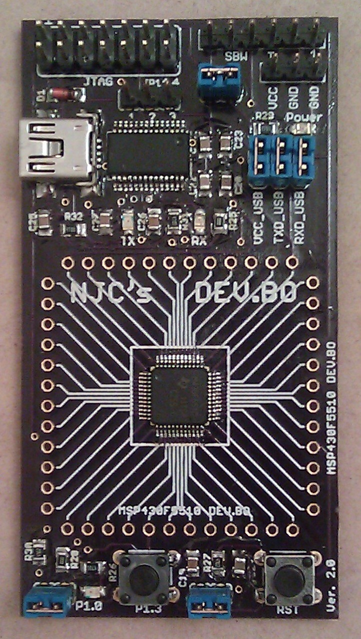
Here I will show you how to build a simple DAC using just the LaunchPad and a few common analog components!
It has been quite some time since I have posted some code and after all that has been going on I now have time to write a new technical post! Though I developed this mini-project on the MSP430F5510, I have ported it over to the MSP430G2231 so it can be implemented using just a LaunchPad and some common analog components. This project came about because I wanted to automate signal to noise testing on a product I am making and I did not have the money for a new controllable digital function generator. I needed a way generate a sine wave, then I needed to sweep across a certain small range of frequencies. At each frequency data would be logged and then analyzed in MATLAB.
Sounds complicated, but the principle is very simple. I wanted to build a digital to analog converter (DAC) using an MSP430 that can generate periodic waveforms. I came up with this concept and decided to build it mostly out of curiosity since I could have just bought a signal generator chip or high-speed DAC at a very low cost.
This post will show you how to generate a periodic analog signal using the LaunchPad and the MSP430G2231. For the sake of simplicity, I stuck to the default DCO value. This will allow us to generate a very clean sine wave at 128Hz. If the DCO is increased to 16MHz and a few other design parameters are changed the maximum frequency can be over 4kHz. Using the MSP430F5510 I was able to generate a crystal clear 32kHz sine wave.
Why would you want to do this? Well, this code can be modified so any arbitrary analog waveform can be generated (reasonably speaking). At the very least you will learn some interesting analog principles if you decide to build this mini-project.
How it Works
First I will start out with some theory. The goal here is to generate an analog sine wave (or any signal for that matter). An analog signal, or a continuous signal, is not something which a microcomputer easily works with unless there are analog peripherals to make the job easy. Even then, things are quite discrete. The figures below show a continuous sine wave, and a discrete sine wave.
This is very basic theory, feel free to skip ahead to the code. As you can imagine, the more discrete points per period, the more it looks like a continuous sine wave. The minimum points needed (theoretically) to represent a certain frequency is two (see aliasing). In order to have a clean representation of the signal though, quite a few more than two points are needed. For this post I have chosen to use 32 points per period to make a sine wave for the sake of simplicity. This actually can be reduced which will allow for greater speeds while maintaining very good signal quality.
Great, now we know how to make an analog signal from a few analog points, but how do we generate these analog points in time? PWM. If you are unfamiliar with PWM, please check out an old post of mine here and the wiki page. By using a digital PWM signal, an analog voltage can be generated which is determined by the duty cycle of the PWM. If you take the average voltage across a single period of PWM by using a capacitor (or low-pass filter) a range of analog values can be generated.
So now we can generate the 32 analog points of our sine by using PWM with a little bit of analog circuitry.
The Code
Before we get to the analog circuitry I thought I would discuss the code first. As always, the code is posted here on github and is embedded below.
First, I would like to discuss the sine wave look-up table which is at the top of the code. The array is called wave[] and consists of the 32 values we need to make a sine wave. It is important to note that even though we have 256 possible duty cycles when using 256 clock pulses per PWM, we never go above 192 or below 64 (for a range of 128). This is very important since all of the instructions which need to get executed every interrupt take clock cycles of their own. If the duty cycle interrupt happens before the other interrupt routine finished, a pulse is missed and the output signal becomes warped.
The code itself is quite simple because we are simply generating a PWM using interrupt routines. Again, if this code seems very foreign to you, please check out my post on PWM. The important difference between this code and the typical PWM code is that the duty cycle automatically is changed every period.
Every time a new period is started, the interrupt TIMERA0_VECTOR is thrown. Here will increment a counter which keeps place of our position in the sine wave array; we also will reset the counter as needed. The current value which we are going to be outputting is set to the Capture Compare Register 1 (CCR1). Though it is possible to clear or set the output pin without going into an interrupt routine, I thought it was important to show how the CCR1 interrupt is call because it is slightly different than CCR0.
A separate interrupt vector, TIMERA1_VECTOR, is thrown when the timer is equal to the value in CCR1. This is also the interrupt vector that is called for any other CCR registers that may be available on the MSP430 and overflows. For example, the MSP430F5510 has a timer with 7 capture compare registers! To determine which register threw the interrupt you must check the TAIV register. To see which bit corresponds to which capture register, see the datasheet for your device.
Other than that, if you have read my other posts, you should understand the code. If you have any questions, you know the drill.
The Analog Circuitry
The PWM signal will need to be average, or smoothed out. If the high frequency components are removed, only the average signal remains. Lets make a quick example before we get to the physical implementation on a breadboard.
The above image shows a rectified sine wave which is made up of multiple higher frequency sine waves (blue). This will allow us to visualize how filtering works. After filtering the signal using a low-pass filter, which allow only the frequencies lower than the desired rectified sine wave through; realistically it is not a perfectly sharp cutoff and a little low amplitude high frequency components remain. The result is shown above in green. If this is a bit hard to understand, do not worry, this is just some background theory for those who are interested. Now, let me show you what our actual PWM output will look like for a sine wave.
The above image shows what our PWM output will actually look like. You can see that there are 32 separate PWM periods which make up the sine wave. Each PWM period consists of 256 clock ticks; thus the final sine wave consists of 32*256 = ~8k clock ticks. The final sine wave output is also shown above in green. This is the result of filtering the PWM output signal. For those who are wondering, all of the graphs above were generated in MATLAB.
The Circuit
Great! Now we know how it all works, but how do we actually implement it. I will skip out on filter theory and just present you with a second order low-pass filter
Above is the schematic for all of the analog circuitry that is needed. The analog output, when using the code show above, from the MSP430 will be centered at approximately half of the supply voltage. If we wanted to amplify the signal further, we would need a reference voltage for any amplifier circuitry. For this project we will not do that for the sake of simplicity.
Now onto the circuit. It consists of two passive, low-pass filters separated by two voltage followers (buffers). While it is possible to simply cascade the two filters without the buffers, buffers allow impedance matching; a topic which I will not discuss here. Each filter has a cufoff frequency of approximately 160Hz ( 1/(2*pi*10k*.1uF) ) which is slightly above the desired sine wave frequency of 128Hz and much less than the PWM frequency of 4kHz (1MHz/256 clock ticks).
Note: If you change the timing of the microcomputer to allow for faster or slower sine waves, you MUST also change the cutoff frequency of the low-pass filters.
The Results?
What does the output look like? This post wouldn’t be complete without some scope captures to show the actual results. I really love when the theory works out and the results can be seen easily. Understanding the theory behind not only digital systems, but also analog circuitry can be a huge help in all sorts of projects.
The above image shows both the PWM output from the MSP430 and the sine wave output from the low-pass filters. Very cool! As you can see, the peak to peak voltage of the sine wave is less than the supply voltage (VDD, which is ~3.6V).
The picture above allows you to better see the sine wave output which is 1V peak to peak and 131Hz; it sure looks great! To improve the results, some changes can be made to the project. Less points can be used per sine wave, thus increasing the maximum frequency generated. This makes the output more “jagged” but with correct filtering this would not matter. Further, if you want to increase the peak-to-peak voltage or increase the power for any reason, amplification can be used.
For all the scope measurements I used a Rigol Oscilloscope (DS1052E) which I discovered through the EEVBlog. It is an amazing scope for the price and I would recommend it to anyone. Personally I think it is much better than the really low end Tektronix which are much more expensive, and I much prefer this to older analog scopes.
Final Thoughts
What’s next? It is possible to change the frequency of the sine wave within the MSP430. This could also be the basis for an arbitrary digital function generated using the MSP430. The possibilities are endless! As always, if you have any questions please comment here or email me. If you want a more immediate answer (since I am busy and sometimes take a while to respond) post your question on 43oh.com/forum. Maybe one day soon I will combine the LaunchScope and this project to create a single, simple, controllable, single test board solution using the DEV.BO.
I hope that you found this interesting. I know you all will come up with many cool uses for this project, so please comment and let me know the cool ways which you use the code.
Sounds complicated, but the principle is very simple. I wanted to build a digital to analog converter (DAC) using an MSP430 that can generate periodic waveforms. I came up with this concept and decided to build it mostly out of curiosity since I could have just bought a signal generator chip or high-speed DAC at a very low cost.
This post will show you how to generate a periodic analog signal using the LaunchPad and the MSP430G2231. For the sake of simplicity, I stuck to the default DCO value. This will allow us to generate a very clean sine wave at 128Hz. If the DCO is increased to 16MHz and a few other design parameters are changed the maximum frequency can be over 4kHz. Using the MSP430F5510 I was able to generate a crystal clear 32kHz sine wave.
Why would you want to do this? Well, this code can be modified so any arbitrary analog waveform can be generated (reasonably speaking). At the very least you will learn some interesting analog principles if you decide to build this mini-project.
How it Works
First I will start out with some theory. The goal here is to generate an analog sine wave (or any signal for that matter). An analog signal, or a continuous signal, is not something which a microcomputer easily works with unless there are analog peripherals to make the job easy. Even then, things are quite discrete. The figures below show a continuous sine wave, and a discrete sine wave.
 |
| Continuous Sine Wave |
 |
| Discrete Sine Wave |
Great, now we know how to make an analog signal from a few analog points, but how do we generate these analog points in time? PWM. If you are unfamiliar with PWM, please check out an old post of mine here and the wiki page. By using a digital PWM signal, an analog voltage can be generated which is determined by the duty cycle of the PWM. If you take the average voltage across a single period of PWM by using a capacitor (or low-pass filter) a range of analog values can be generated.
So now we can generate the 32 analog points of our sine by using PWM with a little bit of analog circuitry.
The Code
Before we get to the analog circuitry I thought I would discuss the code first. As always, the code is posted here on github and is embedded below.
First, I would like to discuss the sine wave look-up table which is at the top of the code. The array is called wave[] and consists of the 32 values we need to make a sine wave. It is important to note that even though we have 256 possible duty cycles when using 256 clock pulses per PWM, we never go above 192 or below 64 (for a range of 128). This is very important since all of the instructions which need to get executed every interrupt take clock cycles of their own. If the duty cycle interrupt happens before the other interrupt routine finished, a pulse is missed and the output signal becomes warped.
The code itself is quite simple because we are simply generating a PWM using interrupt routines. Again, if this code seems very foreign to you, please check out my post on PWM. The important difference between this code and the typical PWM code is that the duty cycle automatically is changed every period.
Every time a new period is started, the interrupt TIMERA0_VECTOR is thrown. Here will increment a counter which keeps place of our position in the sine wave array; we also will reset the counter as needed. The current value which we are going to be outputting is set to the Capture Compare Register 1 (CCR1). Though it is possible to clear or set the output pin without going into an interrupt routine, I thought it was important to show how the CCR1 interrupt is call because it is slightly different than CCR0.
A separate interrupt vector, TIMERA1_VECTOR, is thrown when the timer is equal to the value in CCR1. This is also the interrupt vector that is called for any other CCR registers that may be available on the MSP430 and overflows. For example, the MSP430F5510 has a timer with 7 capture compare registers! To determine which register threw the interrupt you must check the TAIV register. To see which bit corresponds to which capture register, see the datasheet for your device.
Other than that, if you have read my other posts, you should understand the code. If you have any questions, you know the drill.
The Analog Circuitry
The PWM signal will need to be average, or smoothed out. If the high frequency components are removed, only the average signal remains. Lets make a quick example before we get to the physical implementation on a breadboard.
 |
| Example Signal |
 |
| Actual Theoretical Output |
The above image shows what our PWM output will actually look like. You can see that there are 32 separate PWM periods which make up the sine wave. Each PWM period consists of 256 clock ticks; thus the final sine wave consists of 32*256 = ~8k clock ticks. The final sine wave output is also shown above in green. This is the result of filtering the PWM output signal. For those who are wondering, all of the graphs above were generated in MATLAB.
The Circuit
Great! Now we know how it all works, but how do we actually implement it. I will skip out on filter theory and just present you with a second order low-pass filter
 |
| Analog Circuitry |
Now onto the circuit. It consists of two passive, low-pass filters separated by two voltage followers (buffers). While it is possible to simply cascade the two filters without the buffers, buffers allow impedance matching; a topic which I will not discuss here. Each filter has a cufoff frequency of approximately 160Hz ( 1/(2*pi*10k*.1uF) ) which is slightly above the desired sine wave frequency of 128Hz and much less than the PWM frequency of 4kHz (1MHz/256 clock ticks).
Note: If you change the timing of the microcomputer to allow for faster or slower sine waves, you MUST also change the cutoff frequency of the low-pass filters.
The Results?
What does the output look like? This post wouldn’t be complete without some scope captures to show the actual results. I really love when the theory works out and the results can be seen easily. Understanding the theory behind not only digital systems, but also analog circuitry can be a huge help in all sorts of projects.
 |
| Actual PWM Output |
 |
| Sine Wave Output |
For all the scope measurements I used a Rigol Oscilloscope (DS1052E) which I discovered through the EEVBlog. It is an amazing scope for the price and I would recommend it to anyone. Personally I think it is much better than the really low end Tektronix which are much more expensive, and I much prefer this to older analog scopes.
Final Thoughts
What’s next? It is possible to change the frequency of the sine wave within the MSP430. This could also be the basis for an arbitrary digital function generated using the MSP430. The possibilities are endless! As always, if you have any questions please comment here or email me. If you want a more immediate answer (since I am busy and sometimes take a while to respond) post your question on 43oh.com/forum. Maybe one day soon I will combine the LaunchScope and this project to create a single, simple, controllable, single test board solution using the DEV.BO.
I hope that you found this interesting. I know you all will come up with many cool uses for this project, so please comment and let me know the cool ways which you use the code.